
Diamond’s New Scarcity Is Expertise

Lab-grown production made diamond economically feasible for technology. As diamond enters more hardware applications, the expertise needed to specify, produce, and evaluate it is in short supply.
Future Calling

Motorola just dropped a major announcement out of the Qualcomm Tech Summit, and while the mainstream tech press is distracted by camera megapixels and software features, our eyes went straight to the thermal architecture. Why? Because with the newly previewed Motorola Signature 27, the company is bringing advanced diamond material science right to the palm of your hand.
Introducing the LattiSpec Curator Private AI Chatbot

As technology-grade grown diamond (TGGD) transitions from a visionary material to the backbone of next-generation hardware, the bottleneck in adoption is rarely interest—it is technical complexity. Hardware developers in semiconductors, quantum computing, high-power electronics, and defense know the precise operational hurdles their devices face, such as critical thermal throttling or weak signal detection. However, translating those performance requirements into specific diamond crystal specifications, synthesis techniques, and post-growth processing remains a significant hurdle.
To bridge this translation gap and streamline procurement, LattiSpec has officially launched LattiSpec Curator, a specialized private AI chatbot integrated directly into the LattiSpec managed marketplace. Designed specifically for the nuances of advanced diamond technology, LattiSpec Curator acts as an intelligent first point of contact for engineers, buyers, and researchers navigating the platform.
Diamonds After Scarcity

Falling prices are expanding diamond’s use as a material in AI and quantum technology, creating a market where specialized supply must meet application-specific demand.
Breakthrough in Inline Metrology
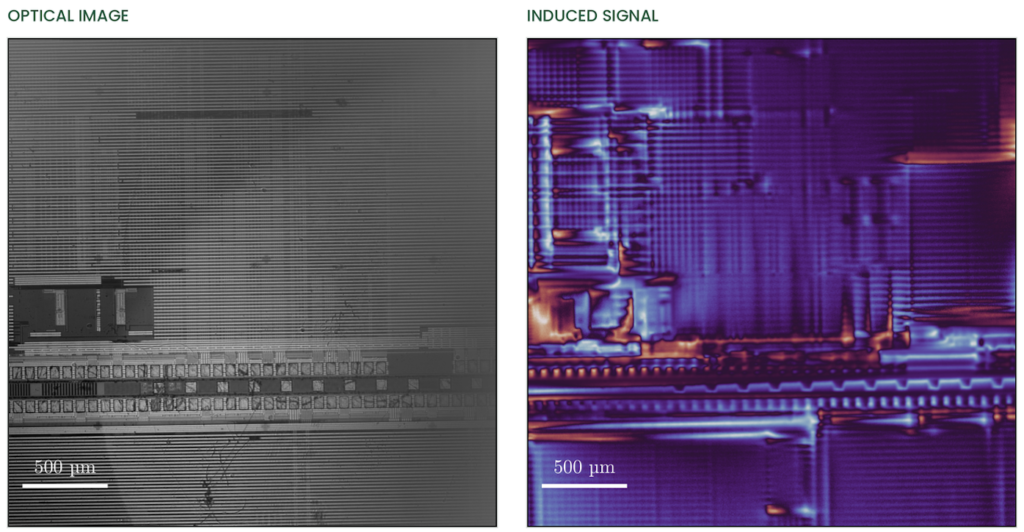
In the world of high-volume semiconductor manufacturing, the leap from the failure analysis (FA) lab to inline inspection is notoriously difficult. For electrical current imaging, that transition has been blocked by a massive bottleneck: the need for a physical connection. Until now, visualizing current flow required wiring up a sample using probe cards, package pins, or exposed pads—a luxury you can afford in an FA lab, but an impossibility on a fast-moving production line.
Driving Innovation with Advanced Materials

Premier Seller Spotlight: Navi Material
Fujitsu develops diamond-spin quantum computer prototype

New diamond-spin quantum computer prototype incorporating tin-vacancy (SnV) centers into photonic integrated circuits marks significant step toward quantum computing scalability.
Microchip Tech with Diamond Cooling

In the relentless push for higher performance in radio frequency (RF) electronics, thermal
dissipation remains the single biggest bottleneck.
The Quantum Opportunity Beyond Computing

Lockheed Martin is helping move quantum sensing from the lab to real-world platforms where precision, resilience and reliability matter most.
Quantum Diamonds Spark a New Era in Particle Physics at Argonne

When it comes to unlocking the deepest secrets of the universe, researchers at the U.S.
Department of Energy’s (DOE) Argonne National Laboratory are turning to an unexpected tool: flawed diamonds.
In a recent press announcement, Argonne unveiled a new three-year, $1 million initiative that will merge the cutting-edge fields of quantum information science and high-energy physics. The project aims to develop next-generation, diamond-based quantum sensors capable of mapping electromagnetic fields with unprecedented precision.

