

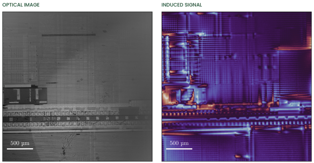
In the world of high-volume semiconductor manufacturing, the leap from the failure analysis (FA) lab to inline inspection is notoriously difficult. For electrical current imaging, that transition has been blocked by a massive bottleneck: the need for a physical connection. Until now, visualizing current flow required wiring up a sample using probe cards, package pins, or exposed pads—a luxury you can afford in an FA lab, but an impossibility on a fast-moving production line.
But earlier this month at SEMICON Taiwan, Munich-based quantum sensing company QuantumDiamonds (QD) announced a milestone that could change the game.
The company successfully demonstrated a novel method for imaging electrical current inside a semiconductor structure without making any physical contact. This achievement removes the primary constraint that has kept quantum-sensing-based current imaging off the factory floor, paving the way for high-volume inline inspection.
Ditching the Galvanic Connection
Any technique that images current must first make the current flow. Rather than relying on a direct electrical bias (a galvanic connection), QD’s new method excites the current electromagnetically using microwave fields.
These induced currents generate microscopic magnetic fields. QD’s proprietary diamond quantum sensors measure these magnetic fields directly, reconstructing them into a high-resolution map of where current is—and isn’t—flowing. What’s particularly promising is that this measurement utilizes the exact same diamond sensor head found in QD’s commercial QDm.1 FA system. The proven sensing hardware working in today’s FA labs is already primed to be ported into an inline configuration.
With extraordinary thermal conductivity ranging from 1,200 to over 2,200 W/mK, CVD diamond farsurpasses traditional metals like copper or aluminum. These thermal substrates are typicallymanufactured in standard thicknesses from 0.2 mm to 2.5 mm, with surface flatness tightly controlled tobelow 4 μm/cm. In addition to heat transfer, they feature excellent electrical insulation, a low coefficient ofthermal expansion (CTE), and high chemical stability
A Critical Missing Link for Advanced Packaging
As we frequently cover here at LattiSpec, advanced packaging techniques like hybrid bonding and stacked 3D architectures are burying interconnects deep within devices, rendering them completely out of reach. Furthermore, measuring an unpowered, unfinished, mid-process wafer stack makes physical electrical excitation impossible. Contactless excitation is the only viable option.
This is where QD’s new technique fills a massive industry void. An interconnect might pass a structural inspection, proving it is physically intact, but still fail to carry an electrical current.
Dr. Fleming Bruckmaier, CTO of QuantumDiamonds, summarized the distinction perfectly: “Acoustic imaging tells you whether a structure is mechanically sound. We tell you whether current is actually moving through it. Those are different questions, and a package can pass one and fail the other.”
Because the diamond sensor naturally maps the 3D field vector of the induced current signature, the technique also allows for depth reconstruction—pinpointing exactly where a failure occurs within a multi-layered stack.
The Trade-Off: Whole-Field vs. Isolated Traces
Like all metrology techniques, this new approach carries a specific trade-off. Because the microwave excitation couples into the entire field of view at once, it images everything simultaneously. It cannot isolate a single trace in the way that selectively biasing a specific test pad can.
However, for interrogating a mid-process wafer with zero electrical access, isolation isn’t the goal. Surveying the entire structure in a single, whole-field acquisition is exactly what the industry needs to maintain production speeds.
Offering fine particle sizing from 5 nm up to 1 μm, these materials feature a unique flaky polycrystallinestructure. Unlike traditional monocrystalline diamond, this polycrystalline structure is designed to microfracture during the polishing process, continually exposing fresh, sharp cutting edges. This selfsharpening mechanism ensures aggressive, efficient material removal while delivering a highly uniform,sub-nanometer surface finish—critically avoiding the subsurface damage common with other abrasives
What’s Next?
According to QuantumDiamonds CEO Kevin Berghoff, the market demand is already palpable, with manufacturers eager to put their own samples in front of the new tool. Top foundries and packaging customers are currently evaluating the technique on their own die- and package-level samples.
With patents filed, QD is now turning its attention toward optimizing the system’s throughput to meet the rigorous demands of high-volume manufacturing environments.
For metrology and inspection professionals keeping an eye on the transition to advanced 3D packaging, QD’s contact-free current imaging is undoubtedly a milestone to watch.


