


We are thrilled to spotlight Navi Material as one of our Premier Sellers on the LattiSpec marketplace. Operating at the frontier of advanced materials science, Navi Material (navimaterial.com) specializes inthe research, development, and manufacturing of high-performance Chemical Vapor Deposition (CVD) diamond components and precision diamond slurries. You can explore their extensive offerings andrequest custom specifications directly on their LattiSpec Seller Hub.
As modern technology—from next-generation electric vehicles (EVs) to aerospace optics—pushes the boundaries of thermal, optical, and mechanical endurance, standard materials are increasingly becoming performance bottlenecks. Navi Material addresses these critical challenges with engineered syntheticdiamond solutions designed to thrive under extreme conditions. Below, we explore their core productlines and the technology sectors that heavily rely on them.
1. CVD Diamond Heat Spreaders & Thermal Substrates
Managing heat dissipation remains one of the most significant engineering challenges in high-powerelectronics. As components become smaller, denser, and more powerful, the inability to effectivelyremove heat limits overall system performance and degrades component lifespan. Navi Material’spolycrystalline and single-crystal CVD diamond heat spreaders offer a definitive solution to this thermalbottleneck.
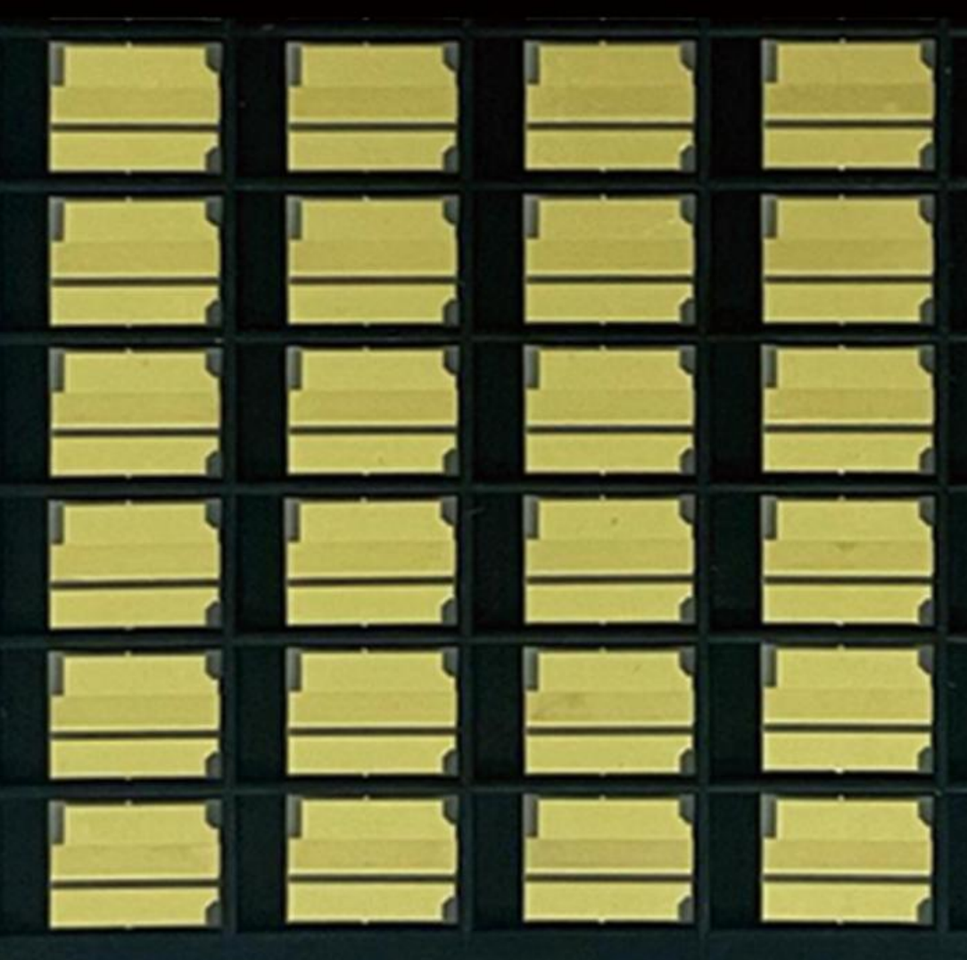
With extraordinary thermal conductivity ranging from 1,200 to over 2,200 W/mK, CVD diamond farsurpasses traditional metals like copper or aluminum. These thermal substrates are typicallymanufactured in standard thicknesses from 0.2 mm to 2.5 mm, with surface flatness tightly controlled tobelow 4 μm/cm. In addition to heat transfer, they feature excellent electrical insulation, a low coefficient ofthermal expansion (CTE), and high chemical stability
KEY TECH INDUSTRY SECTORS
– Telecommunications & 5G: Essential for Gallium Nitride (GaN) and RF power modules wherethermal overload can cause severe signal degradation and hardware failure.
– Semiconductors & AI: Extensively used in advanced chip packaging and AI accelerator chips torapidly draw heat away from densely packed, high-frequency transistors.
– Aerospace & Defense: Deployed in high-power radar and microwave electronics that operate inextreme environments where system reliability is paramount.
2. CVD Diamond Optical Windows
For optical systems that operate under intense radiation, elevated temperatures, or harsh environmentalexposure, standard glass, quartz, or sapphire windows can quickly fail. Navi Material supplies high-puritypolycrystalline and single-crystal CVD diamond optical windows engineered specifically to meet theseextreme demands.
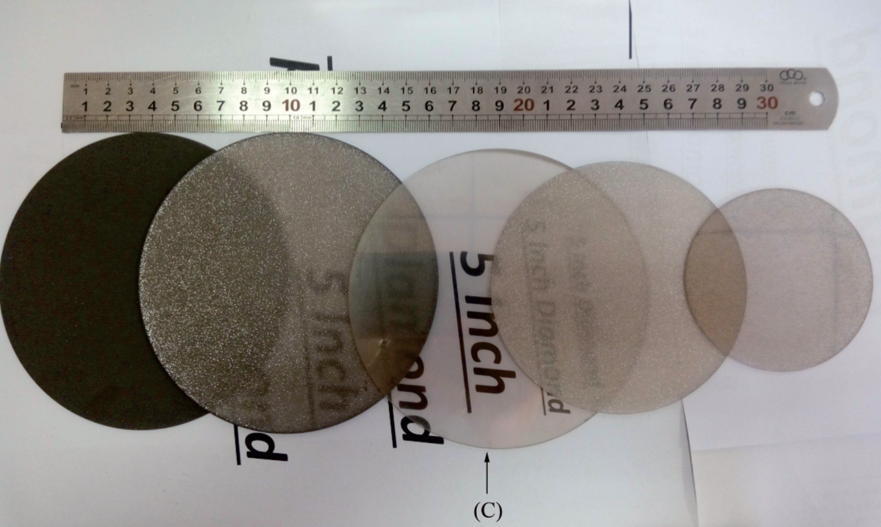
The defining characteristic of these optical windows is their exceptional broad-bandwidth transmission,providing uncompromised transparency from ultraviolet (UV) all the way through infrared (IR) and intomicrowave frequencies. Combined with the extreme hardness and high thermal shock resistanceinherent to diamond, these windows maintain their structural and optical integrity even when subjected torapid thermal cycling, intense localized heating, or mechanical abrasion.
KEY TECH INDUSTRY SECTORS
– Laser Technology: Indispensable for high-power laser systems (such as industrial CO2 lasers andmedical lasers) where the window must transmit intense energy without absorbing heat orfracturing.
– Defense & Space Exploration: Utilized in IR and microwave optical setups, as well asmultispectral sensor systems operating in space or harsh terrestrial environments.
– Advanced Manufacturing: Used as highly durable viewports in vacuum process chambers andcorrosive chemical processing environments.
3. Polycrystalline Nano Diamond Powders & Polishing Slurries
Achieving damage-free, ultra-smooth surfaces is a strict prerequisite for advanced photonics, wafermanufacturing, and advanced ceramics. Navi Material provides precision-engineered polycrystallinediamond powders and ready-to-use slurries optimized for Chemical-Mechanical Planarization (CMP) andsub-nanometer surface finishing
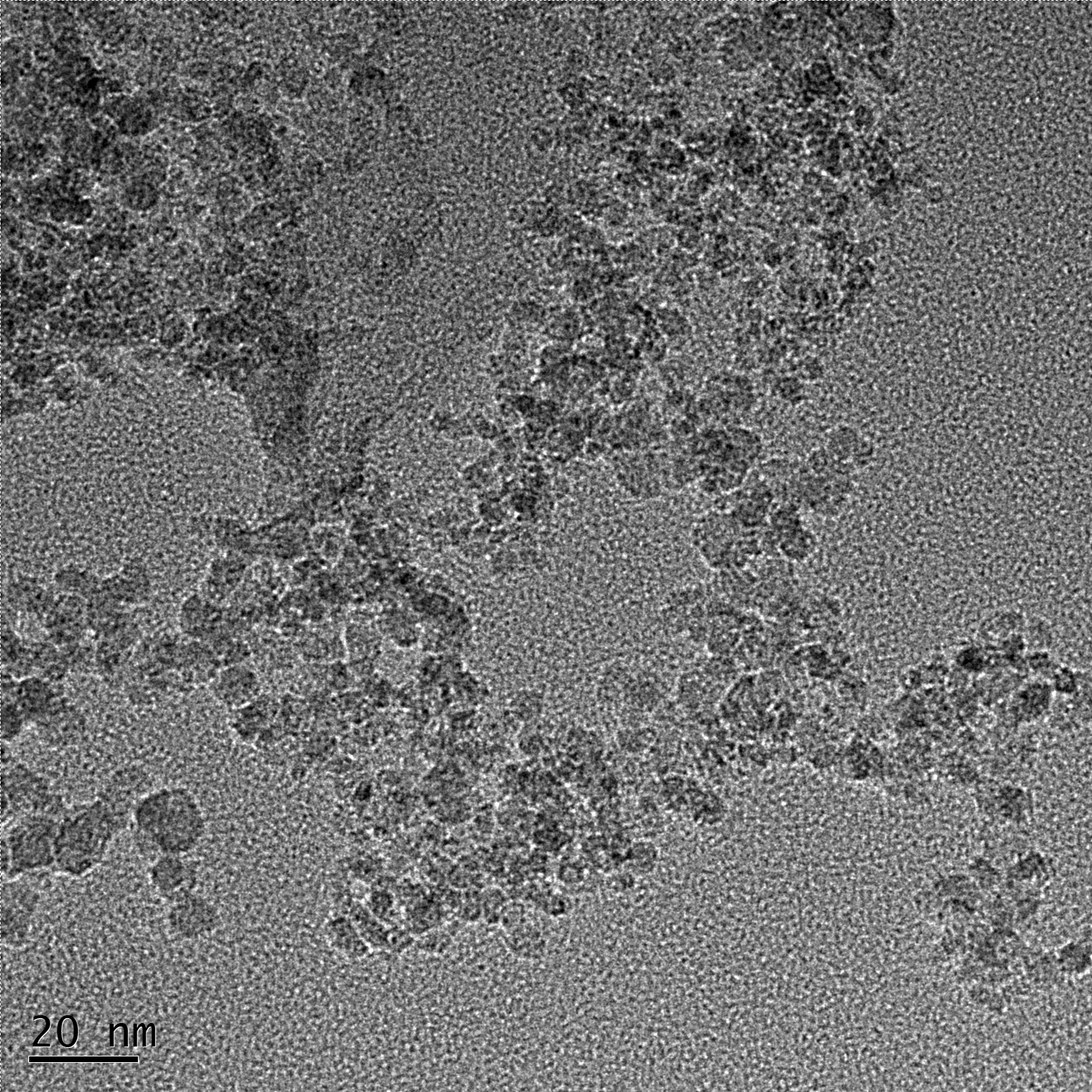
Offering fine particle sizing from 5 nm up to 1 μm, these materials feature a unique flaky polycrystallinestructure. Unlike traditional monocrystalline diamond, this polycrystalline structure is designed to microfracture during the polishing process, continually exposing fresh, sharp cutting edges. This selfsharpening mechanism ensures aggressive, efficient material removal while delivering a highly uniform,sub-nanometer surface finish—critically avoiding the subsurface damage common with other abrasives
KEY TECH INDUSTRY SECTORS
– Semiconductor Manufacturing: Crucial for the precision lapping and polishing of hard-to-processsubstrates like Silicon Carbide (SiC) and Gallium Nitride (GaN) wafers, which are foundational toEV power electronics.
– Photonics & Optics: Employed in laser crystal polishing and finishing optical substrates whereeven microscopic surface imperfections could scatter light or reduce efficiency.
– Advanced Ceramics: Used to achieve ultra-precise, scratch-free finishes on structural ceramicsand metallographic testing samples.
Empowering the Next Generation of Tech
Whether you are designing advanced thermal management systems for the latest AI accelerators,engineering high-power laser optics, or perfecting the surface finish of next-generation semiconductorwafers, Navi Material brings verified, world-class material quality to the table. Their ability to customizeparticle size, surface modifications, and substrate dimensions makes them an invaluable partner fordeep-tech innovation.We invite all buyers, engineers, and supply chain managers to explore Navi Material’s comprehensiveproduct listings and request custom specifications directly through their LattiSpec Hub: lattispec.com/store/navi-material/.


