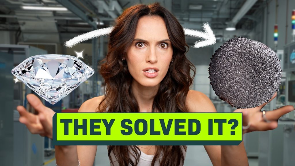
Why Intel’s CEO is Betting on Tech Diamond Packaging
The physics of advanced semiconductor scaling has hit a wall, and it isn’t an optical lithography problem—it’s a thermal one.
As AI workloads reshape computing architectures, the spotlight is shifting from transistor density to packaging efficiency. Speaking recently on the No Priors podcast, Intel CEO Lip-Bu Tan underscored this exact paradigm shift, highlighting that the primary bottlenecks in the AI expansion era are infrastructure-driven: power conversion, advanced packaging, and heat dissipation. To address the latter, Tan revealed a highly strategic personal bet on material science: an investment in Tech Diamond wafer pioneer Diamond Foundry.
The Copper Bottleneck
For decades, the industry relied on copper and aluminum to draw heat away from active silicon. But as high-bandwidth memory (HBM) stacks tighten around hyper-dense GPUs and accelerators, traditional thermal interface materials (TIMs) are failing to dissipate heat fast enough. The result is thermal throttling—chips forcing themselves to slow down to prevent physical damage.
To keep performance scaling linearly, the industry requires a material with a radically higher thermal conductivity. Enter technology-grade grown diamond.
| Material | Thermal Conductivity (W/m·K) | Relative Performance |
|---|---|---|
| Silicon | ~150 | Baseline substrate |
| Aluminum | ~205 | Standard cooling components |
| Copper | ~400 | Traditional high-performance heat sinks |
| Tech Diamond | >2,000 | 5x better than copper |
Why Diamond Foundry?
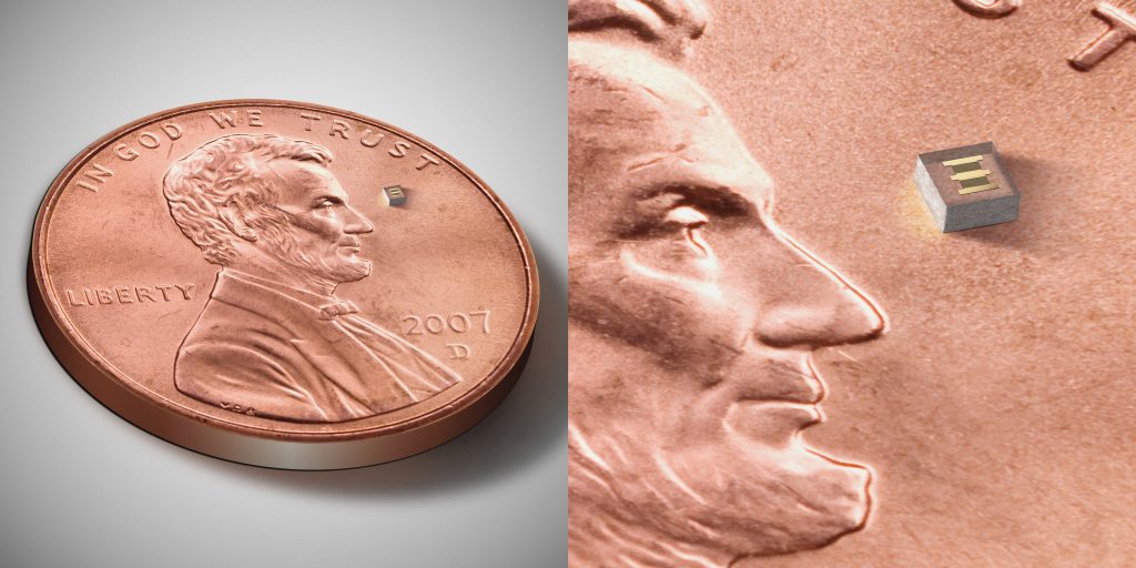
While the concept of using diamond as a semiconductor heat sink is not new, manufacturing it at a scale and cost viable for chip packaging has been notoriously difficult. Diamond Foundry has made waves in the industry by leveraging a proprietary plasma reactor technology to grow single-crystal diamond wafers.
By utilizing Chemical Vapor Deposition (CVD), the firm can create large, atomic-level sheets of diamond. In advanced chip packaging, a diamond substrate can be integrated directly behind the hot spots of an ASIC or GPU, acting as an extreme thermal spreader that pulls heat away instantly.
“Future AI competition will not only occur in hyperscale data centers,” Tan noted during his discussion on industry bottlenecks. The expansion of Agentic AI, reinforcement learning, and edge computing will demand maximum token value per watt, meaning every milliwatt saved on cooling translates directly to compute efficiency.
What it Signals for the Foundry Landscape
Tan’s focus on Diamond Foundry highlights a broader trend: the convergence of venture capital strategy and massive industrial execution. As Intel aggressively pushes its 18A process and builds out its advanced packaging ecosystems, identifying these deep-tech materials bottlenecks early is vital.
While the investment is personal, it serves as a massive validation for diamond’s roadmap in the semiconductor supply chain. For architectural engineers and hardware designers, the message from the top is clear: the next breakthrough in chip performance won’t just come from the silicon foundry—it will come from the materials lab.
To hear more about how shifting AI workloads are restructuring global semiconductor supply chains, check out this Bloomberg interview detailing Lip-Bu Tan’s strategic playbook. This video provides context on Tan’s broader initiatives to revitalize manufacturing culture and address hardware bottlenecks since taking the helm at Intel.