
Navi Material
Kowloon, HK
CVD Diamond (Chemical Vapor Deposition)

CVD Diamond

$50 — $100,000
USD / unit / piece
Built-to-order
Ships in NA
Quantity
units
Range $50 — $100,000
Request a Quote

Compare

No technical specifications added yet.

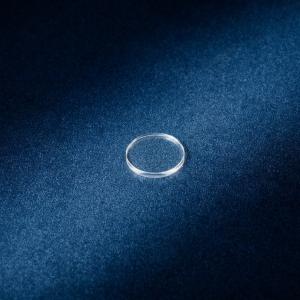
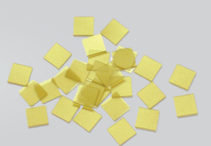
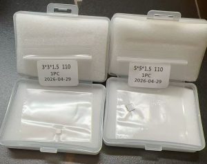
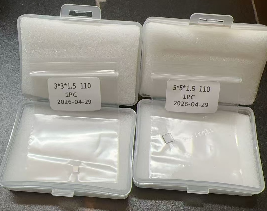
  • Our integrated CVD diamond substrate series covers all mainstream industrial grades, including electronic-grade single crystal diamond blanks with customizable (100)/(110)/(111) crystal orientation like the 3×3×1.5mm and 5×5×1.5mm polished substrates displayed, thermal-conductive polycrystalline heat spreaders, high-transmittance optical windows, NV quantum sensing single crystal wafers, boron-doped conductive BDD electrode plates and wear-resistant CVD tool blanks.
    All CVD materials are manufactured by advanced vapor deposition equipment in our Taiwan production base, with optional double-sided ultra-polishing, ultra-flat finishing, titanium/gold/platinum metallization, laser cutting, drilling and hetero-bonding with Si, Cu, Mo and SiC substrates. The full lineup features ultra-high thermal conductivity up to 2200 W/mK, wide-spectrum optical transmittance, ultra-low internal defects, excellent chemical inertness and adjustable boron doping concentration for conductive electrode use.
    These CVD diamond substrates are widely applied in GaN radio frequency chips, SiC power modules, high-power laser optical systems, quantum magnetic sensing, industrial electrochemical wastewater treatment and precision non-ferrous metal cutting. We support fully customized size, thickness, crystal orientation and surface processing, with both small lab sample pieces and large-volume industrial bulk supply available for global semiconductor, aerospace, photonics and new energy customers.
  • Thermal Management Heat Spreaders
    Core Material: Poly & Mono CVD Diamond
    Key Specifications: Thermal Conductivity 1200–2200+ W/mK; Thickness 0.2–2.5 mm; Flatness <4 μm/cm
  • Optical Windows
    Core Material: Poly & Mono CVD Diamond
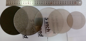
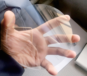
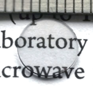
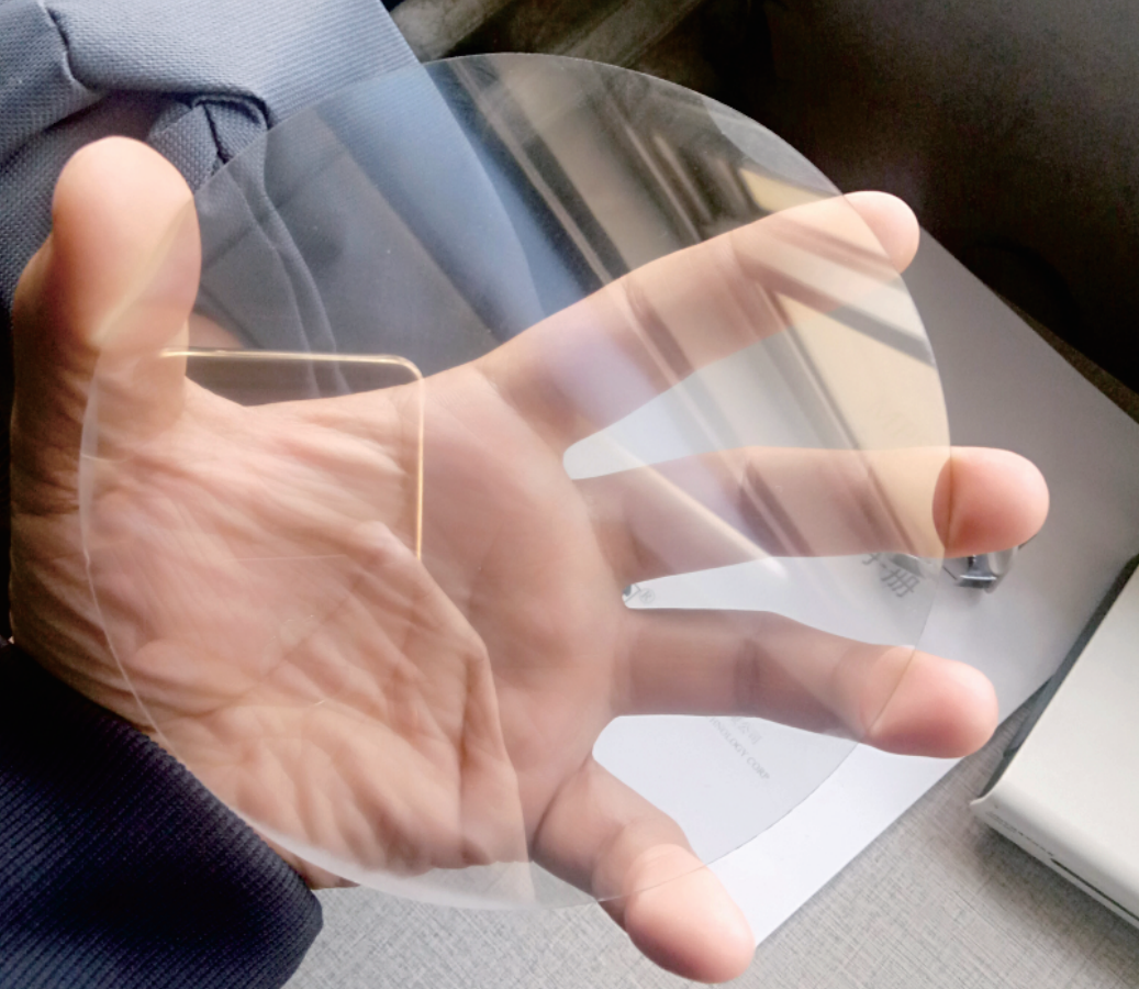
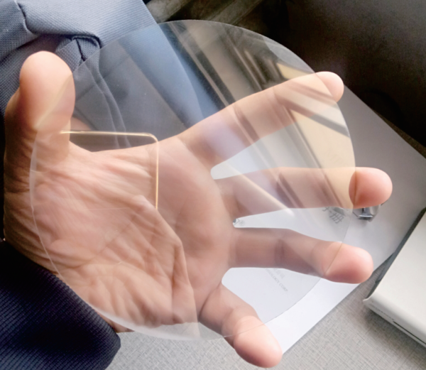
    Key Specifications: Max Diameter 127 mm; Thickness 0.3–3 mm; IR Transmission @10.6μm >70%; Ra <10 nm
  • Electronic Grade Mono Diamond Substrates
    Core Material: Mono CVD Diamond
    Key Specifications: Size 3–10 mm+; Thickness 0.04–4 mm; Orientation (100)/(111)/(110); Nitrogen level 0.01–1 ppm
  • Quantum & Sensing NV Grade Diamond
    Core Material: Mono CVD Diamond
    Key Specifications: Customizable nitrogen vacancy (NV) center engineering
  • Electrochemical Boron Doped Diamond (BDD)
    Core Material: B-doped CVD Diamond
    Key Specifications: Max Diameter 100 mm; Thickness 0.3–2 mm; B Concentration 2×10²⁰–6×10²⁰ atoms/cm³
  • Precision Machining Tool Blanks
    Core Material: Poly CVD Diamond
    Key Specifications: Hardness 8000–10000 kg/mm²; Thermal Conductivity >1000 W/mK

No documents attached yet.

Leave a Review

Your email address will not be published. Required fields are marked *

Shipping Information
OriginKowloon, HK
Lead TimeNA
IncotermsEXW
InsuranceIncluded
TrackingReal-time · door-to-door
Export & Compliance
RoHSCompliant (2015/863)
REACHNo SVHC >0.1%
Navi Material

Navi Material

Navi Material specializes in the research and production of advanced materials, including various types of Grown Diamonds.

Our primary focus is on nano and micron powder technology, which enables us to provide precise and high-performing materials that are crucial to our clients' success.

We cater to industries such as semiconductors, optics, ceramics, composites, and metallography, offering customized solutions to meet their specific needs.

At Navi Material, we are more than just a supplier; we are your partner in progress, providing cutting-edge materials to help your business thrive.

Kowloon, HK

Seller Hub

Description

  • Our integrated CVD diamond substrate series covers all mainstream industrial grades, including electronic-grade single crystal diamond blanks with customizable (100)/(110)/(111) crystal orientation like the 3×3×1.5mm and 5×5×1.5mm polished substrates displayed, thermal-conductive polycrystalline heat spreaders, high-transmittance optical windows, NV quantum sensing single crystal wafers, boron-doped conductive BDD electrode plates and wear-resistant CVD tool blanks.
    All CVD materials are manufactured by advanced vapor deposition equipment in our Taiwan production base, with optional double-sided ultra-polishing, ultra-flat finishing, titanium/gold/platinum metallization, laser cutting, drilling and hetero-bonding with Si, Cu, Mo and SiC substrates. The full lineup features ultra-high thermal conductivity up to 2200 W/mK, wide-spectrum optical transmittance, ultra-low internal defects, excellent chemical inertness and adjustable boron doping concentration for conductive electrode use.
    These CVD diamond substrates are widely applied in GaN radio frequency chips, SiC power modules, high-power laser optical systems, quantum magnetic sensing, industrial electrochemical wastewater treatment and precision non-ferrous metal cutting. We support fully customized size, thickness, crystal orientation and surface processing, with both small lab sample pieces and large-volume industrial bulk supply available for global semiconductor, aerospace, photonics and new energy customers.
  • Thermal Management Heat Spreaders

    Core Material: Poly & Mono CVD Diamond

    Key Specifications: Thermal Conductivity 1200–2200+ W/mK; Thickness 0.2–2.5 mm; Flatness <4 μm/cm

  • Optical Windows

    Core Material: Poly & Mono CVD Diamond

    Key Specifications: Max Diameter 127 mm; Thickness 0.3–3 mm; IR Transmission @10.6μm >70%; Ra <10 nm

  • Electronic Grade Mono Diamond Substrates

    Core Material: Mono CVD Diamond

    Key Specifications: Size 3–10 mm+; Thickness 0.04–4 mm; Orientation (100)/(111)/(110); Nitrogen level 0.01–1 ppm

  • Quantum & Sensing NV Grade Diamond

    Core Material: Mono CVD Diamond

    Key Specifications: Customizable nitrogen vacancy (NV) center engineering

  • Electrochemical Boron Doped Diamond (BDD)

    Core Material: B-doped CVD Diamond

    Key Specifications: Max Diameter 100 mm; Thickness 0.3–2 mm; B Concentration 2×10²⁰–6×10²⁰ atoms/cm³

  • Precision Machining Tool Blanks

    Core Material: Poly CVD Diamond

    Key Specifications: Hardness 8000–10000 kg/mm²; Thermal Conductivity >1000 W/mK

Reviews

There are no reviews yet.

Be the first to review “CVD Diamond”

Your email address will not be published. Required fields are marked *

ABOUT

Brand & Company Overview

Legal name
World Elite Investment Limited
Brand name
NAVI MATERIAL

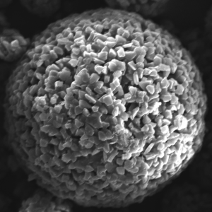
Navi Material is a professional global R&D and manufacturer specializing in micron, nano HPHT diamond materials and full-spectrum CVD diamond products, delivering one-stop advanced diamond material solutions for high-end industrial clients worldwide. Our product portfolio covers etched monocrystalline diamond, spherical & agglomerated diamond powder, high-purity nano diamond, thermal management diamond fillers, plus CVD thermal spreaders, optical windows, electronic substrates, NV quantum diamond, boron-doped conductive BDD electrodes and precision tool blanks.
We own proprietary crushing, shaping, purification and surface etching techniques. Our mechanical-crushed nano diamonds outperform traditional detonation-made counterparts with over 99.8% purity, stable dispersion and eco-friendly mass production. We also offer exclusive waste diamond agglomeration recycling to cut clients’ raw material costs. Our Taiwan CVD facility utilizes advanced deposition reactors and ultra-precision polishing to produce high-conductivity, chemically inert monocrystalline and polycrystalline CVD diamond.
We serve semiconductor wafer polishing, new energy thermal management, aerospace, photonics, quantum technology, precision machining and electrochemical wastewater treatment. Custom services include particle size tuning, surface modification, laser cutting, metallization and substrate bonding. Supported by stable domestic supply chains and a dedicated technical team, we supply dry powder or slurry products globally, acting as reliable technical partners to solve customers’ polishing, grinding and heat dissipation challenges across North America, Europe and Southeast Asia.

CAT

Product Categories

Diamond Material CVD Diamond (Chemical Vapor Deposition) Electronic Grade (High Purity / Low Strain) Diamond Material CVD Diamond (Chemical Vapor Deposition) Optical Grade Single Crystal (High Transparency) Diamond Material CVD Diamond (Chemical Vapor Deposition) Thermal Grade Polycrystalline (High Conductivity) Diamond Components Optical & Laser Components (Optics / Photonics / Defense) CVD Diamond Windows (IR, Microwave, UV)
SPEC

Full Material Specifications

Thermal Conductivity1200u20132200+ W/mK;
VISUALS

Images & Assets

In-situ #1 In-situ #1
In-situ #2 In-situ #2
Schematic Schematic
CAD CAD
SHIP

Logistics & Lead Times

Stock StatusBuilt-to-order
Lead TimeNA
Rush OptionNo
FOB PointHong Kong, China
IncotermsEXW
CONTACT

Technical Contact

Navi Material
Verified LattiSpec Hub Seller

Navi Material specializes in the research and production of advanced materials, including various types of Grown Diamonds.

Our primary focus is on nano and micron powder technology, which enables us to provide precise and high-performing materials that are crucial to our clients' success.

We cater to industries such as semiconductors, optics, ceramics, composites, and metallography, offering customized solutions to meet their specific needs.

At Navi Material, we are more than just a supplier; we are your partner in progress, providing cutting-edge materials to help your business thrive.

Established2014
Responds in8 hrs
LocationChina
View All Products from Navi Material →